Selective laser-induced etching of glass and sapphire

Brochure Selective laser-induced etching of glass and sapphire
© Fraunhofer ILT, Aachen, Germany.
Brochure Selective laser-induced etching of glass and sapphire

The Fraunhofer Institute for Laser Technology ILT has made a manufacturing process available – the two-step »Selective Laser-Induced Etching« (SLE) – that can generate microchannels, shaped holes and cuts and 3D geometric shapes in transparent components made of fused silica, borosilicate glass and sapphire. Micrometer-fine structures and entire components can, thus, be produced directly from 3D CAD designs using a CAD-CAM process chain.

The Process

SLE is a two-step process for manufacturing complex 3D components made of glass or sapphire. In the first step, ultrashort pulsed laser radiation is focused into the volume of the transparent workpiece. The pulse energy is absorbed only in the focus volume based on a multiphoton process. The process modifies the transparent material without cracking it, thereby changing its chemical properties. This way, the material can be selectively chemically etched. By deflecting the focus in the workpiece with a microscanner system, the process can modify contiguous areas. These can be removed in a second process step by means of wet chemical etching, making it possible to produce microchannels, shaped holes, structured components and complex, composite mechanical systems.

Fraunhofer ILT, in collaboration with the Chair for Laser Technology LLT at RWTH Aachen University, has demonstrated for the first time that selective laser-induced etching can be used at process speeds relevant to industry.
Several Advantages of the SLE Process

  • High energy efficiency (remelting instead of evaporation)
  • High material efficiency (kerf of a few microns)
  • High precision in three dimensions (focus < 5 μm, no deposits)
  • Scalability to high productivity, e.g. through high scanning speeds

Economical for Small and Large Series

Since SLE can be scaled down to process times in the range of a few seconds, the industry can utilize it directly. Thus, low-cost components made of various types of glass and sapphire can be produced, components that are not only easily cleaned and sterilized, but also characterized by high durability compared to today‘s plastic components. In the long term, this process has enormous potential for use in individualized mass production, since no expensive masks or molding tools are required and, thus, no component-specific fixed costs are incurred. A component can be generated directly from the software (CAD-CAM chain) within seconds. Therefore, the SLE process enables industrial users to produce prototypes in small and large series and transfer their process parameters easily without needing to readjust them. Furthermore, mechanical microsystems specific to each customer can be manufactured with completely new functional features – while saving costs and time. SLE benefits from virtually unrestricted geometry freedom, taking into account the functional properties for transparent components. With SLE, geometrical shapes can be created that are not feasible with any other process.

Shape Cutting and Shape Drilling

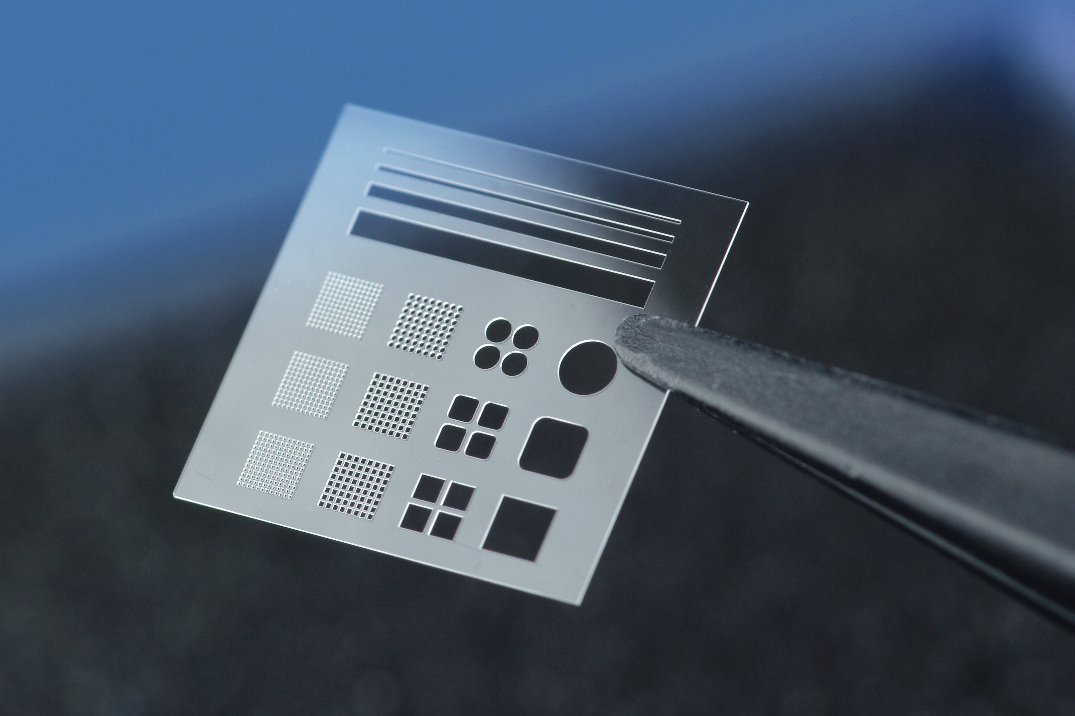
In precision mechanics and medical technology, SLE is already being used to cut out components made of sapphire and glass. Here, for example, it can cut widths of < 5 μm in a material 1 mm thick. As the system has a microscanner and a precise axis system, any shape can be cut with an accuracy of 1 μm. The resulting mold holes and cut components have a surface roughness of the cut edges of Rz < 1 μm. Contour holes < 50 μm and rounded edges with radii < 30 μm were produced in thin glass (< 200 μm, alkali-free borosilicate glass and fused silica).

Microchannels inside Glass and Sapphire

Microfluidic systems can be manufactured with the SLE process in thermally and chemically resistant materials such as fused silica, borosilicate glass or sapphire, for applications in medical diagnostics, among others. In fused silica, the volume modified by the laser is etched 1,000 times faster than in unmodified glass. This selectivity dictates the possible aspect ratios for the microstructures, making, thus, minimum channel diameters of 10 μm at a length of a few millimeters feasible. Channels, branches and any hollow structures can be produced when the laser radiation is scanned or moved inside the material.

Microstructured 3D Components

Currently, any component shape up to a substrate thickness of 14 mm can be produced in fused silica. The SLE process is also suitable for producing microstructured components made of glass or sapphire for precision mechanics such as those used in watchmaking, micro-optics or medical technology. The process can also be used to manufacture microresonators and fiber couplers, and is suitable as a high-precision manufacturing technology for photonic-integrated chips and applications in the field of quantum technologies.

Outlook

Fraunhofer ILT is continuously advancing the SLE process and optimizing it for applications specific to its customers. The institute is focusing on process development to expand the range of materials that can be processed and on scaling up to higher process speeds by using multi-beam technology and new femtosecond laser beam sources with average powers of up to 1 kW.