Microelectronics

The microelectronics industry is increasingly focusing on trend topics such as miniaturization, 3D integration and artificial intelligence (AI). New developments and technologies such as quantum computing will also provide strong impetus for further advances in the medium to long term. With the increased use of mobile devices and the Internet of Things (IoT), energy efficiency is also an important aspect of microelectronics.

Current challenges in microelectronics

Progressive miniaturization on a nanoscale level represents a technological challenge. Ever smaller structures and 2D materials require innovative approaches to overcome current physical limits. Among other things, chips for 5G applications are to be developed that improve connectivity in various application areas – for example, for autonomous vehicles.

Solutions from Fraunhofer ILT

The experts at Fraunhofer ILT develop and evaluate beam sources for EUV lithography and the corresponding measurement technology in order to advance the miniaturization of electronics. In addition to generating structures on the nanometer scale, the institute also focuses on assembly and connection technology for high-performance electronic components. Together with industrial partners, Fraunhofer ILT is developing new connection technologies for battery contacting and power components.

Fraunhofer ILT also has expertise in the structuring and functionalization of surfaces and in 3D volume structuring. For example, microscopic structures can be introduced into glass or sapphire substrates by selective laser etching, structures that can be used to create microfluidic systems for biochemical analyses.


Additively manufactured sensors

In additive manufacturing, sensors can be integrated directly into components thanks to the layer-by-layer building process. This makes it possible to collect load data, a capability that forms the basis for predictive maintenance, big data and AI approaches.


Laser-based packaging

Laser-based packaging securely connects microelectronic components or integrates them solidly into housings. With this innovative approach, components and carrier materials can be joined together precisely and reliably, for example.


Semiconductor technology

Lasers play a central role in semiconductor technology: They structure, process or activate materials. Without precise laser tools, the majority of modern electronic devices and technologies would be inconceivable.

Ansprechpartner

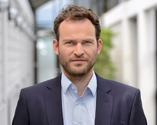
Carlo Holly

Contact Press / Media

Univ.-Prof. Carlo Holly

Head of Department Data Science and Measurement Technology

Fraunhofer Institute for Laser Technology ILT

Steinbachstr. 15
52074 Aachen

Phone +49 241 8906-142

Christian Vedder

Contact Press / Media

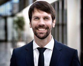
Dr. Christian Vedder

Head of Department Surface Technology and Ablation

Fraunhofer Institute for Laser Technology ILT
Steinbachstr. 15
52074 Aachen

Phone +49 241 8906-378

Hans-Dieter Hoffmann

Contact Press / Media

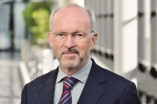
Dipl.-Ing. Hans-Dieter Hoffmann

Head of Department Laser and Optical Systems

Fraunhofer Institute for Laser Technology ILT
Steinbachstr. 15
52074 Aachen

Phone +49 241 8906-206

  • Send email
Alexander Olowinsky

Contact Press / Media

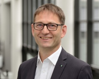
Dr.-Ing. Alexander Olowinsky

Head of Department Joining and Cutting

Fraunhofer Institute for Laser Technology ILT
Steinbachstr. 15
52074 Aachen

Phone +49 241 8906-491

  • Send email
Cancel
  • Kilowatt boost for USP material processing

    Press Release / August 29, 2024

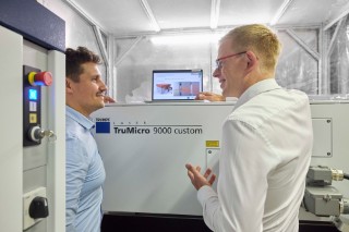
    Steffen Rübling, TRUMPF (left), and Dr. Dennis Haasler, Fraunhofer ILT, discuss details of operating the 1 kW USP laser from TRUMPF.
    © Fraunhofer ILT, Aachen, Germany / Ralf Baumgarten.

    A new ultrashort pulse (USP) laser beam source from TRUMPF, designed for industrial use, will significantly expand the range of applications of USP laser processes. The Fraunhofer Institute for Laser Technology ILT in Aachen will be systematically exploring the potential of this beam source with an average output of 1 kW in the coming months. Among other things, experiments are planned to optimize processes in battery and fuel cell production, toolmaking and semiconductor technology, as well as to test various beam guidance strategies. Many of these pilot applications have their origins in the Fraunhofer internal Cluster of Excellence Advanced Photon Sources (CAPS), to which 21 institutes of the Fraunhofer-Gesellschaft belong.
    more info
  • © Fraunhofer ILT, Aachen.

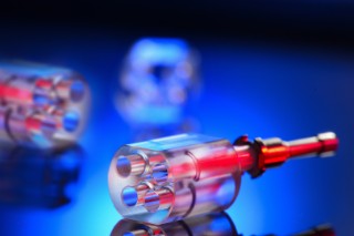
    How pharmaceuticals act, how efficient catalysts are and how effective and accurate printing inks function all depend on the size of the nanoparticles they contain. However, there are as of yet no methods for monitoring the particle size distribution during grinding processes. In the EU-funded PAT4Nano project, a consortium from industry and research has spent the last four years looking for practicable approaches for such inline measurements. The Fraunhofer Institute for Laser Technology ILT in Aachen has developed a promising laser-based method that could soon make such measurements possible.
    more info
  • A look back at the future of photonics

    Review / May 28, 2024

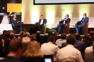
    Discussion round in the Gerd Herziger Session.
    © Fraunhofer ILT, Aachen, Germany / Andreas Steindl.

    The “AKL’24 - International Laser Technology Congress” took place in Aachen from April 17 to 19, 2024. For the 14th time, the congress provided a platform for an intensive professional exchange on current technology trends and perspectives in laser technology. In addition to three forums and nine sessions with a total of 82 specialist presentations, the 525 participants from 21 countries had access to a fully booked exhibition with 58 companies and 60 “Laser Technology Live” demonstrations in the laboratories of the Fraunhofer Institute for Laser Technology ILT and RWTH Aachen University. Two evening events and the deliberately relaxed schedule on the three days of the congress invited participants to network. In short: AKL’24 was the place to be for the laser community.
    more info
  • Laser technology and AI boost the circular economy

    Press Release / March 27, 2024

    Components or modules are analyzed with LIBS in order to secure valuable raw materials in electronic waste. After excitation with a high-energy laser pulse, plasma is formed from which the “atomic fingerprint” of the material can be read using spectroscopy.
    © Fraunhofer ILT, Aachen, Germany.

    The recycling industry is increasingly relying on laser-induced breakdown spectroscopy (LIBS) to identify reusable raw materials in waste streams. The Fraunhofer Institute for Laser Technology ILT in Aachen is playing a leading role in developing this highly precise technology for element analysis and is continuously expanding its range of applications.

    more info
  • AI has the potential to close control loops

    Press Release / January 24, 2024

    "If you close the control loop, you can build a machine that regulates itself. That is the roadmap we are following." Professor Carlo Holly, Head of the Data Science and Measurement Technology Department at Fraunhofer ILT.
    © Fraunhofer ILT, Aachen, Germany.

    Whether in laser material processing, additive manufacturing and repair processes, laser weed control or the automated design of optical systems: Artificial intelligence has enormous, sometimes disruptive potential in photonics. With around 50 international experts in attendance, the 3rd "AI for Laser Technology Conference" took place at the end of November at the Fraunhofer Institute for Laser Technology ILT in Aachen, and clearly showed that the AI-driven transformation is in full swing.

    more info